Ever since I X-rayed the Raspberry Pi 5 to see inside the BCM2712 and RP1 chip packages, I've wanted die shots of both chips. Why? Mostly out of curiosity, since I'm not a silicon expert by any means.
I also ran into some weird overclocking issues after writing about my experience overclocking and underclocking the Raspberry Pi 5, and probably spent an unhealthy amount of time (and money) to learn about the clocks, PLLs, and chips on the latest version of everyone's favorite Single Board Computer.
 (Some Raspberry Pi 5s were harmed in the making of this blog post.)
I get into a lot more of that journey in today's special video for Pi Day (watch it here), but for those who stare far too long at pretty silicon, I have a series of images here, with links to the full images hosted on Siliconpr0n.org.
I donated a number of Raspberry Pi 5's to the cause, along with some funds for the effort, to John McMaster, who did all the actual work delidding, extracting, and etching the silicon to get these images. I also wanted him to share the images on his site like all his other work so anyone can grab full-res copies and dive into this new silicon.
Broadcom BCM2712 SoC die shots
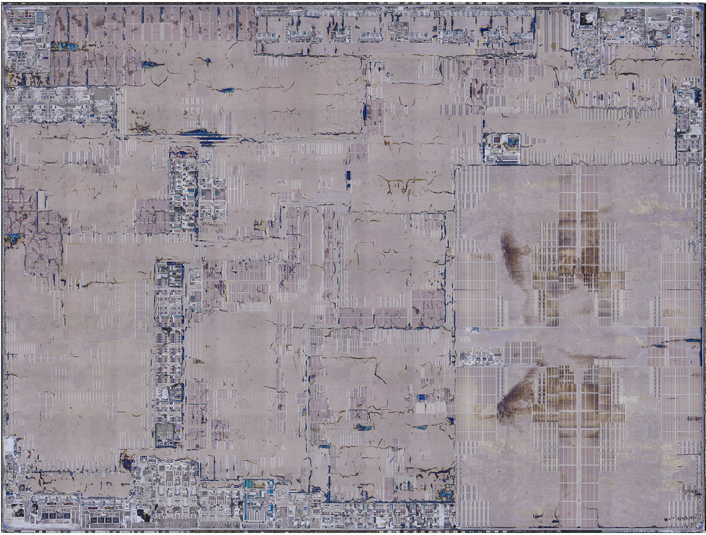
Kicking things off with the BCM2712, this is a modern Arm SoC from Broadcom with 4 A76 cores, an unknown number of GPU cores, at least 5 lanes of PCI Express Gen 2 (capable of Gen 3 but defaults to Gen 2), LPDDR4x DRAM, USB 2.0 (built in), dual 4K HDMI, and a few other interfaces that go unused on the Pi 5 model B, at least.
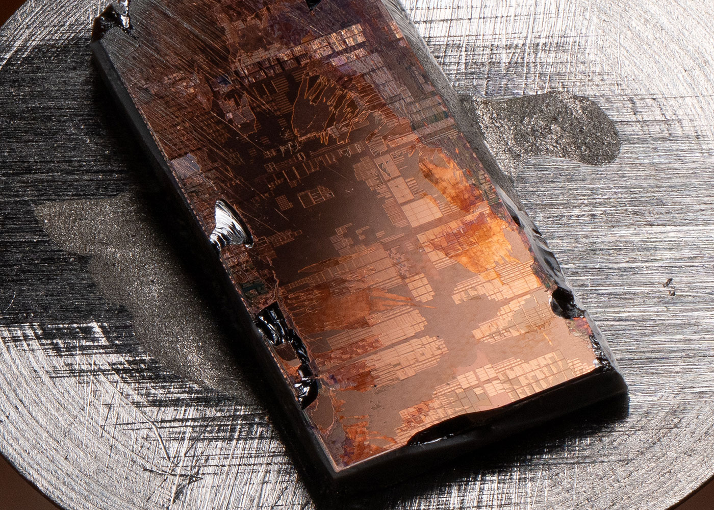
John had a bit of a time getting a clean sample to put under the microscope—I go into the reasons in my video, but eventually we wound up with a clean die, and here's the top layer, which is coated in polyimide, an insulating plastic:
The polyimide is tolerant of very high temperatures, and protects the metal layer beneath from oxidization and potential short circuits. Just like kapton tape, or the protective outer layer of the lunar lander, this layer has a bit of a yellow tinge to it.
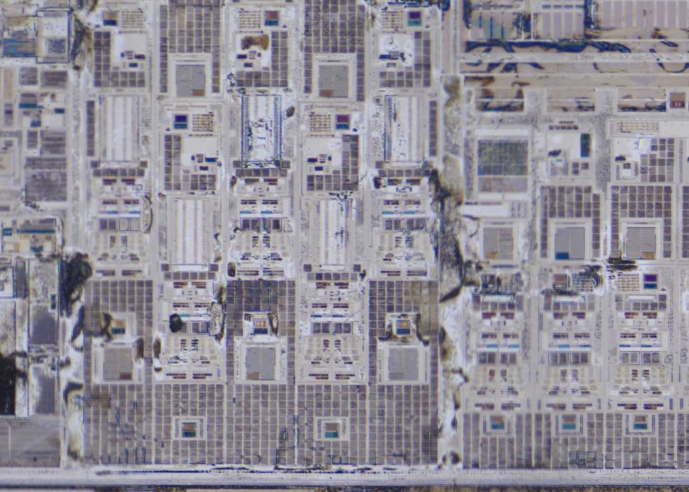
Polishing that off, we get to the metal layer—it looks similar, but more detail is revealed, peering down through the vertical circuit structures that extend from the pads (which connect to the interposer—which then gets soldered to the Pi 5 PCB) all the way down to the silicon:
This layer also shows more clearly some of the features on the relatively thick metal traces embedded above the silicon—some of which I'll touch on soon, but before that, let's move right down to the bare silicon layer, which still shows some remnants of the destructive chemical etching process John had to use to expose it:
And for completeness, I also asked John to expose that layer under different lighting conditions to give more colorful die shot renditions, for example:
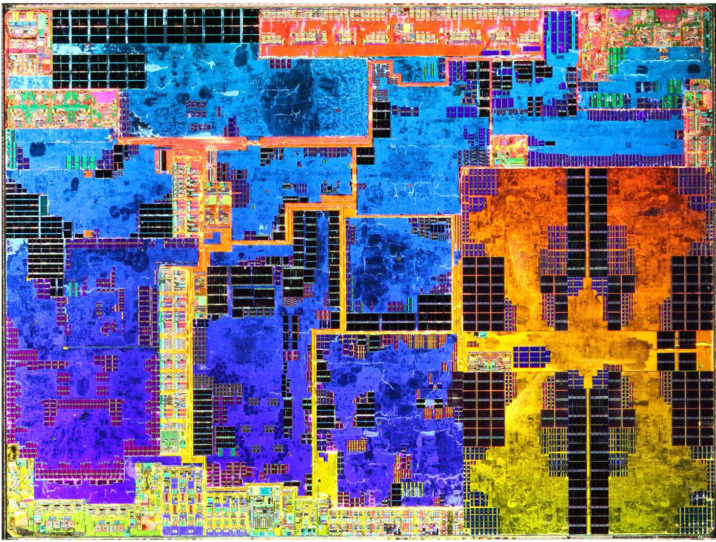
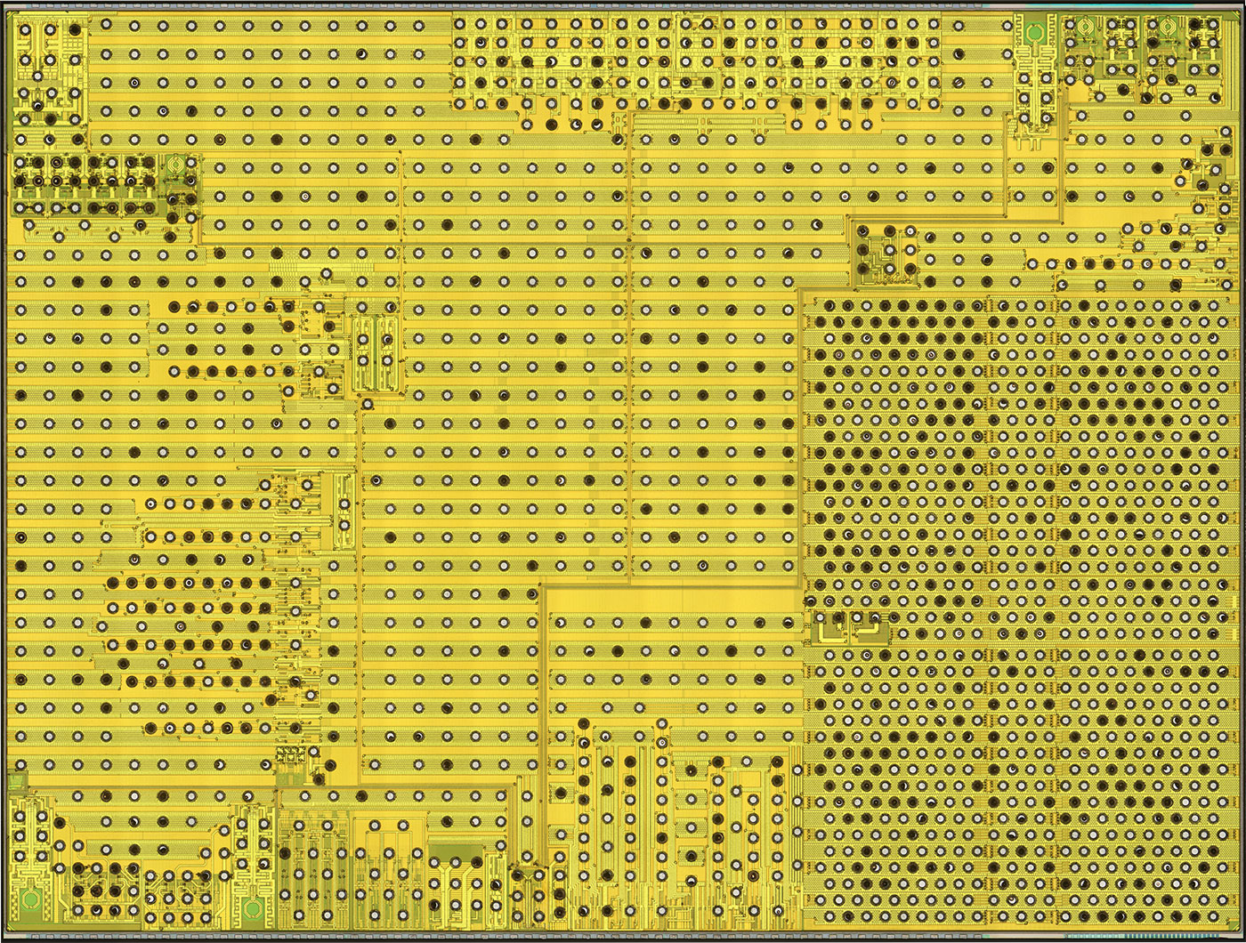
But at this layer, at least one feature on the chip was made very clear—the four Arm A72 cores located towards the bottom right:
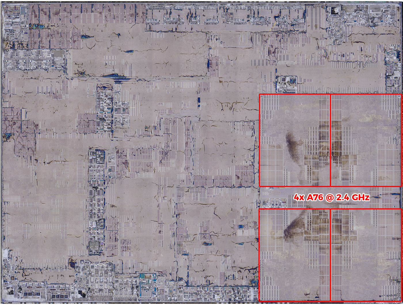
These cores have an integrated 512K L2 cache (per core), and a shared 2MB L3 cache. Over in the open area, there's an integrated 12 core VideoCore VII GPU (not highlighted), among the sea of IO and other areas, for things like HDMI, ISP, HEVC decoding, 6(?) lanes of PCI Express, and all the other dozen or so interfaces this chip exposes.
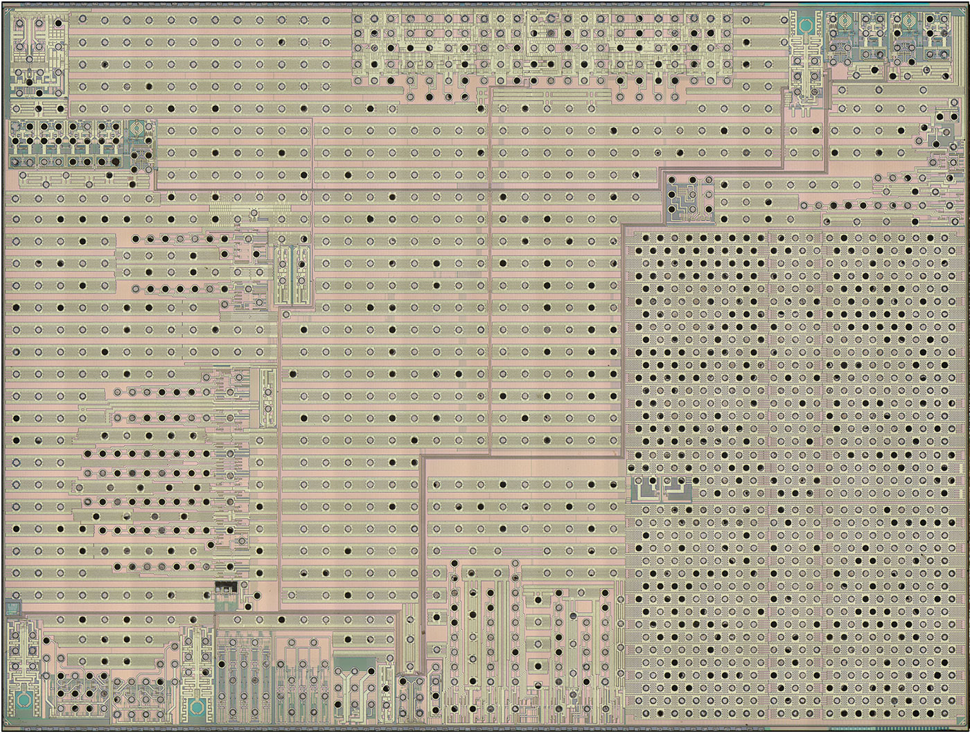
But now, zooming way way in, we can see some details:
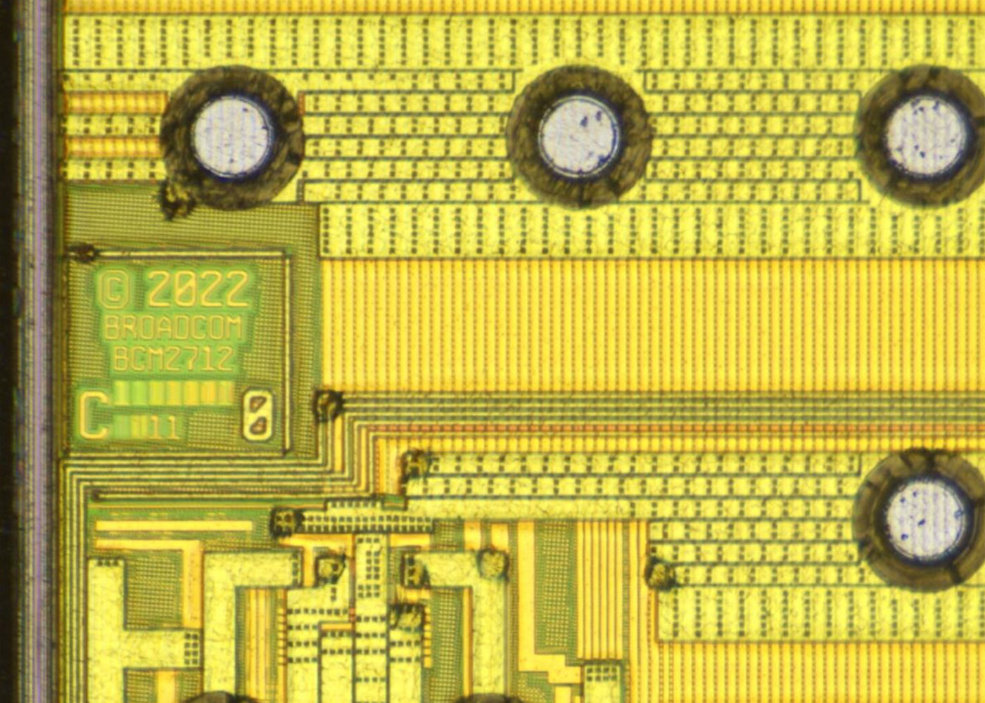
This little portion along the left side shows the stepping (C0, so a third major revision), the design year (2022), the chip name, and a little grid showing various layers above the base silicon. There are 11 '1s' in that grid, so if I'm reading it correctly, there are 11 layers built up on top of the silicon with all the interconnects, to get to this top polyimide layer. Chips are not simple bits of sand!
I'm also fascinated just moving around the chip to spot any interesting details:
This area somehow reminds me of satellite imagery of an industrial, concrete-laden part of town. These seem like IO areas, but maybe they're part of the GPU? Not sure, as I said earlier, I'm no expert on silicon layout or reverse engineering!
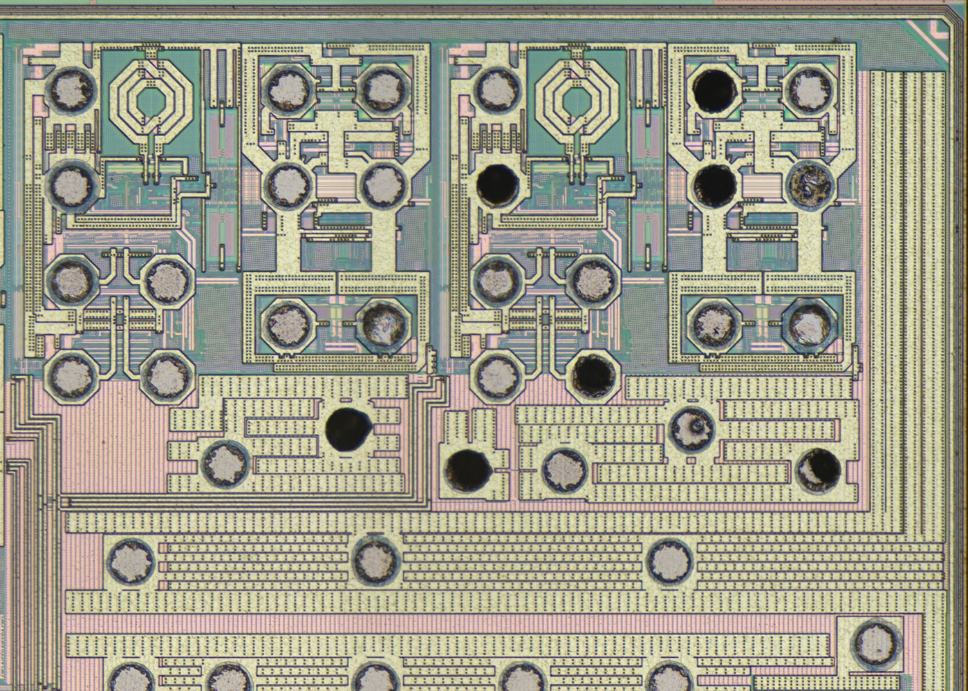
Back up on the metal layer, this was one of my favorite sections, at the top right—those little multi-layer inductors remind me a lot of the Omni Consumer Products / OmniCorp logo from Robocop!
I also spotted a feature that I had to investigate a bit more. I asked the Pi engineers what all those little slightly-tilted dot grids were, seemingly on all parts of the board, in some of the middle metal layers.
Apparently that's Fill, and it's an important part of modern designs, to help with capacitance issues and signal integrity, much like grounding or impedance matching helps with interconnects.
You can spend a few hours scanning over the BCM2712 die shots on Siliconpr0n, but let's move on to RP1, Raspberry Pi's first custom silicon (it was designed well before the RP2, or RP2040, which appears in their Pico microcontroller boards).
Raspberry Pi RP1 die shots
The RP1 is a southbridge chip connecting four PCI Express lanes from the BCM2712 chip to a variety of peripherals, including CSI/DSI, SDIO, DAC, GPIO, I2C, SPI, USB 2.0, USB 3.0, and 1 Gbps Ethernet—it has a lot going on, and really is what makes the Pi a Pi.
If you look at the picture above, you can see in many ways, it's the heart of all the IO for the Pi—a bunch of wires head over from the BCM2712, then the rest of the board to the right of the HDMI jacks is all supplied by RP1!
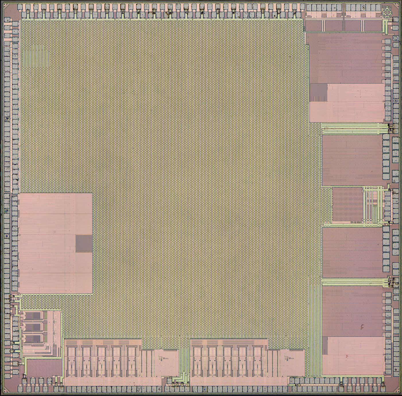
John didn't etch down to the bare silicon on this chip (maybe he or someone else will someday!), but you can see the chip has a smaller count of features than the bigger BCM2712. It's also at 40 nm (versus the SoC at 16 nm), meaning individual transistors and traces are a little larger—but still nowhere near large enough to spot with your typical optical microscope!
![]()
Zooming way in on the top right corner, there's a cute pixel-art Raspberry Pi logo.
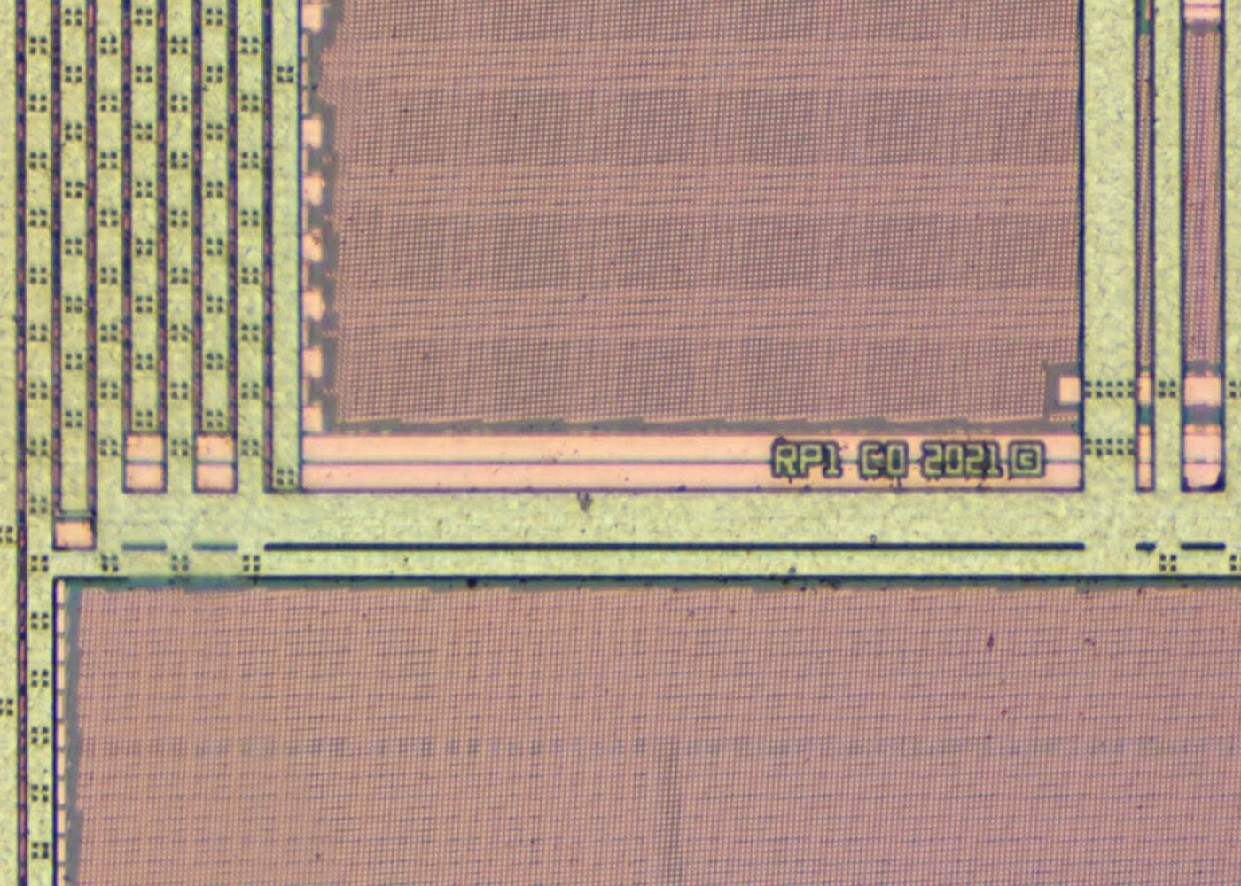
And towards the middle of the right side, this chip shows it was on a C0 stepping back in 2021—so it's a chip Raspberry Pi's invested a lot of time and $25 million into launching.
But with either of these chips, John's (excellent) microscopes can only give a broad overview of the incredibly tiny details on the surface. As chip features approach the size of DNA (like a thousand times smaller than a single human hair), you need much more exquisite tools.
Transistor-level debugging on the BCM2712
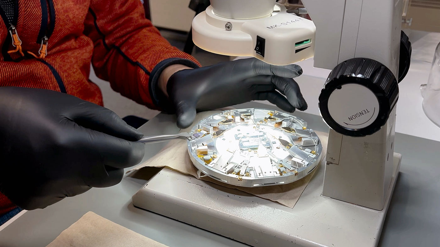
There's more detail in the video, but I worked with a couple engineers at Kleindiek Nanotechnik in Germany to image and test individual transistors on the BCM2712.
After processing the silicon—a destructive process which in this case ran into a few unexpected quirks, like layers of the chip coming apart like a book!—Andreas loaded the chip into one of their probe shuttles, which is inserted into a Scanning Electron Microscope (SEM):
The probes are piezoelectrically-controlled, and can be precisely moved in 0.05 nm increments—on the order of a single atom! This precision is helpful when silicon chip designers need to go into very deep levels of transistor and circuit debugging.
By the time they get to this stage, companies like NXP or Intel will have already run a chip through other debug processes, from a debug socket that narrows down specific blocks to investigate, to OBIRCH ("Optical Beam Induced Resistance CHange"), which uses lasers to prod different parts of the chip and check for anomalies.
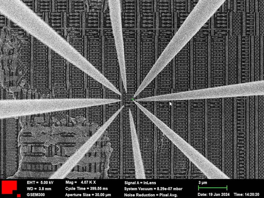
The chip is now inside the electron microscope's vacuum chamber, and after a plasma burns off any remaining organic contaminants that may have made it through earlier sample prep, the probes are positioned over an area of investigation (above).
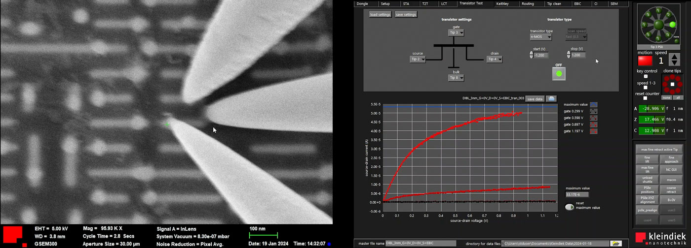
The technician can finally position three of the probes over a transistor's source, gate, and drain, and apply voltage sweeps—measured here in femptoamps. Luckily, the transistors we probed on the Pi 5 were all functioning nicely, despite the way the metal layers delaminated themselves!
Conclusion
The video has more details, but I wanted to also summarize things (and provide a bunch of the still images) in this blog post for those who enjoy sitting with some images of new silicon.
The RP1 is an interesting chip, too, and we can already see the revision on the Pi 5 was finalized in 2021, a couple years before the Pi 5 was released. Raspberry Pi's been working on that chip for years, and have invested $25 million in it. I'd love to see where their in-house silicon team goes from here—or some of the other interesting avenues this new southbridge opens up...
Comments
According to the DTS it's 6 PCIe Gen3 lanes BCM2712 is capable of: https://github.com/raspberrypi/linux/blob/2d3d2030c0564790a76cf94fa0ca1…